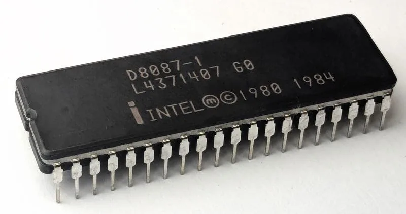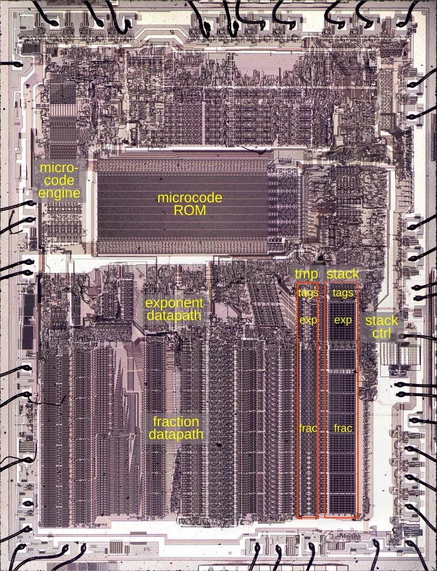
Intel introduced the 8087 floating-point co-processor chip in 1980 to accelerate floating-point operations by up to 100 times [1, 2]. The chip’s design significantly influenced the floating-point standard used by most modern processors [1, 2].
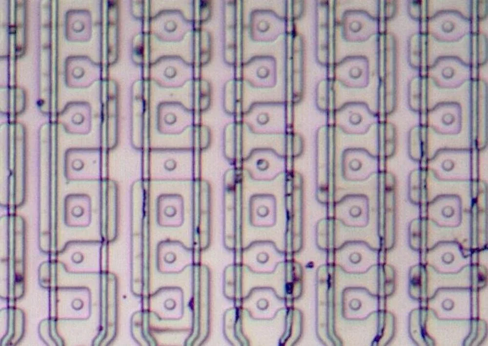
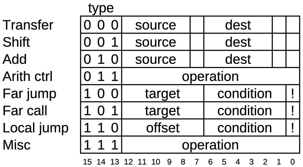
Reverse engineering performed by the Opcode Collective involved opening an 8087 chip and capturing high-resolution microscope images to decode the internal microcode [1, 2]. This revealed the chip contains a large microcode ROM with 1,648 micro-instructions, each 16 bits long, that govern the complex floating-point computations [1, 2].
The microcode engine executes these instructions, handling jumps and subroutine calls to implement operations such as square roots, tangents, and exponentials using sophisticated algorithms embedded in microcode [1, 2].
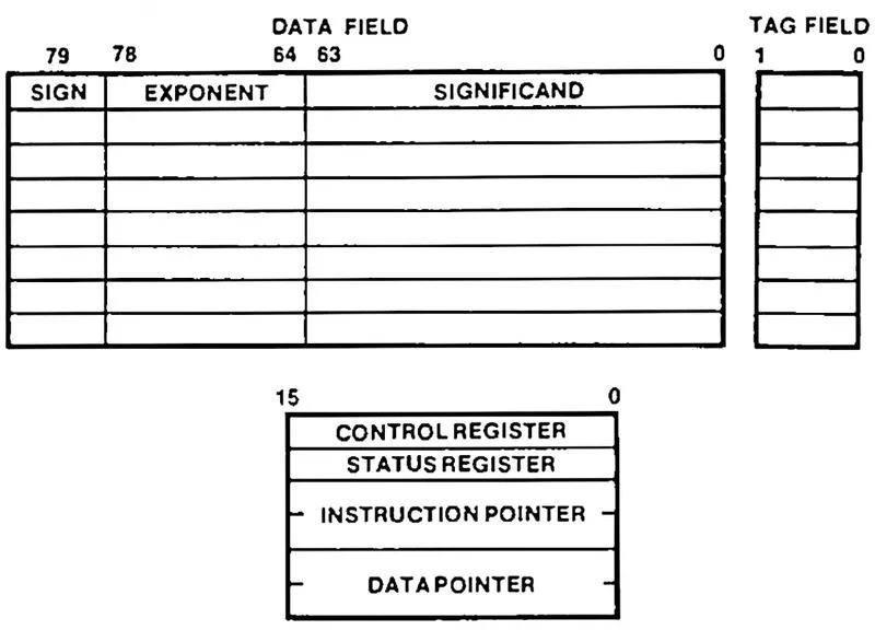
One example of the chip’s complexity is the FXCH (Floating-point Exchange) instruction, which swaps two floating-point registers using 14 micro-instructions [1, 2]. The chip’s datapath divides the floating-point number into a 16-bit exponent path and a 64-bit fractional path (significand) to handle calculations precisely [1, 2].
The 8087 features two temporary registers and eight stack registers. Each register holds both the exponent and fractional parts, along with two tag bits to label the type of value stored [1, 2]. Stack control circuitry manages the top-of-stack position to support push and pop operations on data [1, 2].
In May 2026, Ken Shirriff published a detailed blog post analyzing the 8087’s microcode and instruction implementations, providing valuable insights into this early floating-point co-processor [1, 2].